
|
|
We explore the electrical and optical properties of devices containing atomically precise structures with sizes reaching typically only a few nanometers. In these conditions, charge carriers have to travel through extremely confined geometries, electronic energy levels separate beyond the thermal energy, even at room temperature, and quantum effects become apparent in electrical transport.
Fabricating electronic devices with atomic precision is extremely challenging: disorder, defects and the mobility of individual atoms play an important role at the nanometer scale. While these aspects can be limiting factors in terms of reproducibilty, structural variability at the nanoscale also reveals the richness of microscopic states that can be explored in these devices.
To some level, molecules or also self-assembled metallic and semiconducting clusters can be seen as the smallest building blocks where structure and electronic function can be engineered. Molecules however can be chemically synthesized with atomic precision and in large quantities. Instead of preparing solid-state devices by continuously reducing their size, we therefore combine here micro- and nano-fabrication techniques with chemical bonding and self-assembly to build molecular devices. In such devices, the major electrodes and contact lines are continuous, metallic or semiconducting materials while the smallest, electronically active units are partially or fully organic.
The fabrication and study of molecular devices is a highly interdisciplinary endeavor mixing physics, materials science, chemistry and engineering.
Our fields of research:
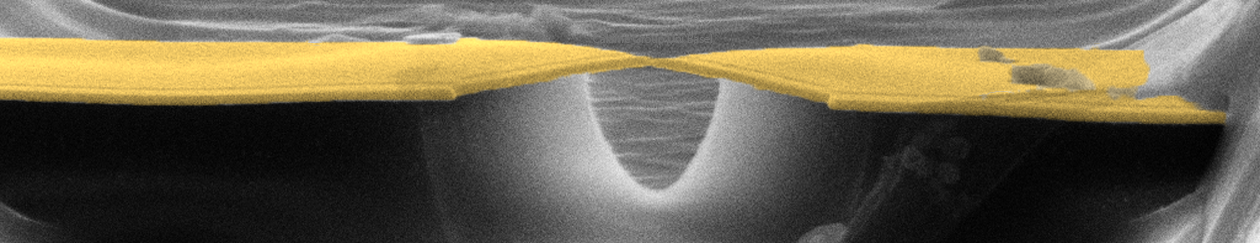
- Mechanically controlled break junctions − an approach for contacting and electrical characterization of individual molecules;
- Silicon Nanowires for (bio-)sensing;
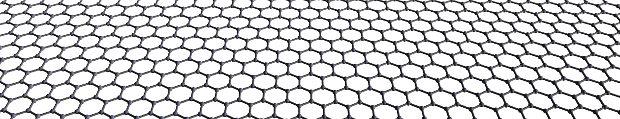
- CVD grown graphene for quantum metrology;
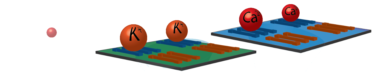
- Graphene nanogaps to contact individual molecules;
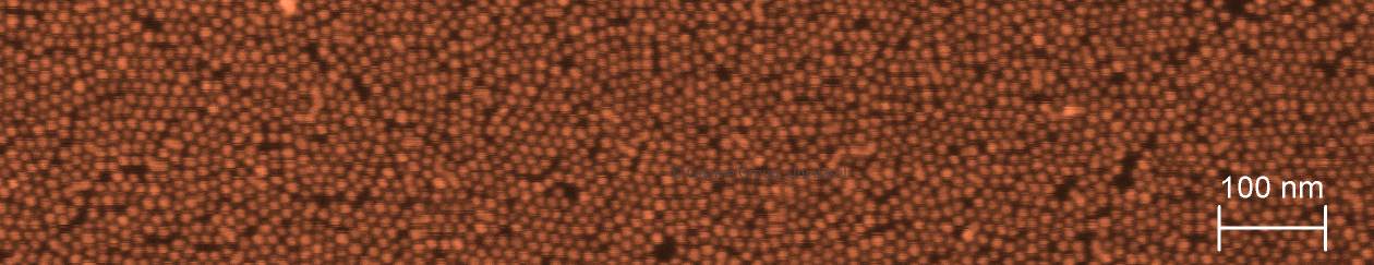
- Nanoparticle arrays as an upscaled platform to investigate properties of the molecules.