
The Transport at Nanoscale Interfaces Laboratory at Empa has an opening for a PhD Student in nanophysics and thermoelectricity
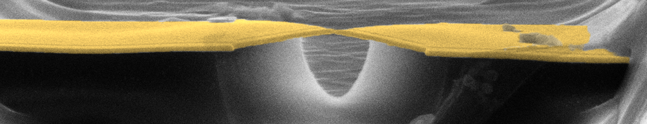
The aim of the project is to design and fabricate molecular junctions with enhanced ability to convert waste heat to electricity making use of quantum interference. For this purpose, room-temperature quantum interference effects will be exploited at the single-molecule level, with the outlook of integration in massively-parallel molecular arrays. The PhD student will be a part of a highly interdisciplinary European project that brings together internationally leading scientists from four different countries. He/she will develop expertise in the areas of nano-fabrication, molecular charge transport, electrical characterization and data analysis.
We are looking for a highly motivated PhD student with a strong background in (nano) physics, physical chemistry and/or material science. Excellent communication skills and fluency in English (both written and oral) are mandatory.
The work will be carried out under supervision of Prof. Dr. Michel Calame. The position will be available from February 2018 on, with a planned project duration of four years.
The working place will be at Empa in Dübendorf, which offers a highly stimulating research environment with state-of-the-art facilities and a broad interdisciplinary surrounding. The PhD student will have access to the advanced nanofabrication facilities available at the Center for Micro- and Nanoscience, ETH Zürich (FIRST lab) and at the Binnig and Rohrer Nanotechnology Center (BRNC), located at IBM Zürich laboratories.
We look forward to receiving your online application including a letter of motivation, CV, diplomas with transcripts and contact details of two referees.
Applications via email will not be considered.


 Congratulations to Anton for successfully defending his PhD thesis entitled “Detailed analysis of single molecular junctions for novel computing architectures.”.