 We systematically investigate the impact of granularity in CVD graphene films by performing Raman mapping and electrical characterization of single (SD) and multi domain (MD) graphene. In order to elucidate the quality of the graphene film, we study its regional variations using large area Raman mapping and compare the G and 2D peak positions of as-transferred Chemical Vapor Deposited (CVD) graphene on SiO2 substrate. We find a similar upshift in wavenumber in both SD and MD graphene in comparison to freshly exfoliated graphene. In our case, doping could play the dominant role behind the observation of such upshifts rather than the influence due to strain. Interestingly, the impact of the polymer assisted wet transfer process is the same in both the CVD graphene types. The electrical characterization shows that SD graphene exhibits a substantially higher (a factor 5) field-effect mobility when compared to MD graphene. We attribute the low sheet resistance and mobility enhancement to a decrease in charge carrier scattering thanks to a reduction of the number of grain boundaries and defects in SD graphene.
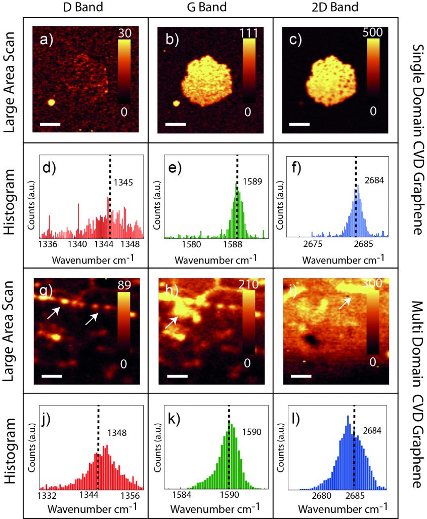
Figure Large area Raman scans of D, G and 2D bands (a-c, g-i) and peak position-histograms of SD (d-f) and MD (j-l) graphene. The average peak positions are marked with black dotted lines for D, G and 2D bands. Features in the large area scans are marked using white arrows. Scale bars: 4 µm (SD) and 2 µm (MD)
Comparative study of single and multi domain CVD graphene using large area Raman mapping and electrical transport characterization
Kishan Thodkar, Maria El Abbassi, Felix Lüönd, Frédéric Overney, Christian Schönenberger, Blaise Jeanneret and Michel Calame
pss-RRL (2016), DOI: