Workshop on Molecular Scale Electronics will be organized by Prof. Dirk Guldi on September 24-27 in Muggendorf near Erlangen, Germany
ECME-2017, Dresden, August 29 − September 2, 2017
14th European Conference on Molecular Electronics (ECME) will be held in Dresden on August 29 – September 2 2017.
ICMSE, Basel, August 27-29, 2017
From August 27 to 29, 2017 NCCR MSE is organizing the first biannual International Conference on Molecular Systems Engineering (ICMSE) in Basel. The ICMSE is a unique event in the emerging field of molecular systems engineering, and has the potential of leading to a long-term paradigm shift in molecular sciences. The three-day conference will be held at the University of Basel (Kollegienhaus, Petersplatz 1).
ICMAT 2017, Singapore, June 18-23, 2017
9th International Conference on Materials for Advanced Technologies will take place on Jun 18-23 in Singapore.
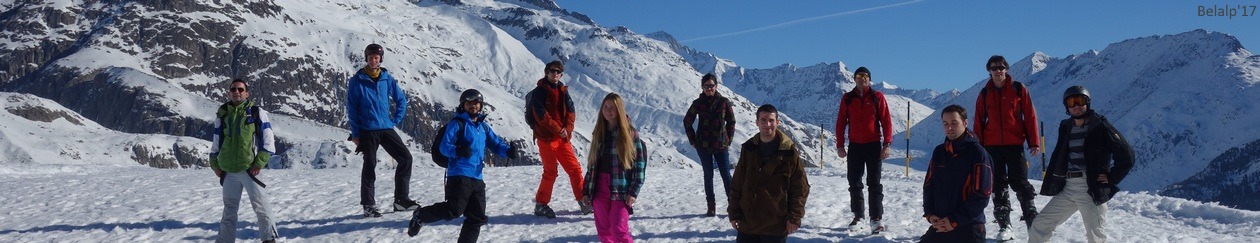
Swiss Nano Convention, Fribourg, June 1-2, 2017
The Swiss Nanoconvention 2017 will be organized in Fribourg on June 1-2, together with the CTI-Micro/Nano event, which focusses on short to medium-term applied science, as well as the NRP64 Final Event.
MOLESCO Workshop, Lancaster, UK, May 15-19, 2017
2017 MOLESCO Workshop on Molecular Electronics will be organized by Colin Lambert on May 15-19 in Lancaster, United Kingdom.
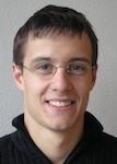
Welcome Mathias and Mickael!
We are happy to welcome two new postdocs in our group.
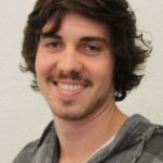
Dr. Mathias Wipf during his doctoral (2010-2014, University of Basel) studies and postdoctoral research job (2015-2016, Yale University, Mark Reed group) worked with silicon nanowire based sensors.
Dr. Mickael Perrin was working in the field of single molecular junctions (as PhD student in 2011-2015 and as a postdoctoral researcher in 2015-2016 at Delft Technical University in the group of Herre van der Zant).
MOLESCO 3rd Annual meeting, Granada, January 17-21, 2017
MOLESCO 3rd annual meeting and workshop will be organized by Michel Calame and Nicolás Agraït on January 17−21, 2017 in Granada, Spain.
QuEEN workshop, Oxford, December 18−20, 2016
QuEEN workshop
From 18th to 20th of December Michel and Maria were invited to the QuEEN workshop on Quantum effects in molecular junctions, organized by Prof. Andrew Briggs et al.
Michel talked about stochasticity in molecular devices.