Just accepted: Charge noise in organic electrochemical transistors

Congratulations to Ralph Stoop and Michele Sessolo. Their paper on “Charge noise in organic electrochemical transistors” will appear in Phys. Rev. Applied.

Abstract

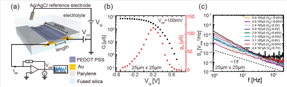
Organic electrochemical transistors (OECTs) are increasingly studied as transducers in sensing applications. While much emphasis has been placed on analyzing and maximizing the OECT signal, noise has been mostly ignored, although it determines the resolution of the sensor. The major contribution to the noise in sensing devices is the 1/f noise, dominant at low frequency. In this work, we demonstrate that the 1/f noise in OECTs follows a charge-noise model, which reveals that the noise is due to charge fuctuations in proximity or within the bulk of the channel material. We present the noise scaling behavior with gate voltage, channel dimensions and polymer thickness. Our results suggest the use of large area channels in order to maximize the signal-to-noise-ratio
(SNR) for biochemical and electrostatic sensing applications. Comparison with literature shows that the magnitude of the noise in OECTs is similar to that observed in graphene transistors, and only slightly higher compared to Carbon nanotubes and Silicon nanowire devices. In a model ion-sensing experiment with OECTs, we estimate crucial parameters such as the characteristic SNR and corresponding limit of detection.


Device schematic and measurement setup for the noise characterization. (b) Conductance G (black, left axis) and transconductance gm(red, right axis) versus liquid gate potential V_lg measured for a 25 um x 25 um OECT. (c) Power spectral density of the voltage fluctuations S_V versus frequency f for the OECT in (b) gated to different conductance values as given in the legend. The black dashed line indicates a 1/f dependence. The scattering peaks are due to the intrinsic noise of the power line matching 50 Hz and multiples of it.


Charge Noise in Organic Electrochemical Transistors
Ralph L. Stoop, Kishan Thodkar, Michele Sessolo and Henk Bolink, Christian Schonenberger and Michel Calame
to appear in Phys. Rev. Applied

Trends in micro nano event in Bienne

On Oct. 25th, the Trend in Micro Nano event organized by the Swiss mnt network took place at the Innocampus in Bienne.  Among other speakers reporting about applied research or applications, we reported there on our work with Silicon-based biochemical sensors and its potential for applications.


Congratulations to Jan for the Best Poster award on the SNI Annual event.

Jan Overbeck with SNI Best poster award - 2016
Jan Overbeck won SNI Best poster award – 2016

In September 2016, SNI members met for their third annual conference in Lenzerheide, where 80 participants were treated to a diverse mixture of lectures and posters to encourage scientific exchange. 

Jan Oberbeck, an SNI doctoral student from Michel Calame’s group, won over the audience with his poster, for which he picked up a prize. 

Press release


Just accepted: paper on single and multi-domain CVD graphene by Kishan Thodkar et al.

fig2
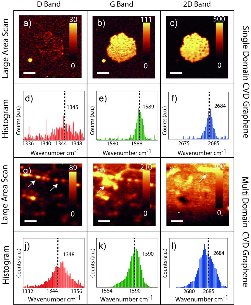
We systematically investigate the impact of granularity in CVD graphene films by performing Raman mapping and electrical characterization of single (SD) and multi domain (MD) graphene. In order to elucidate the quality of the graphene film, we study its regional variations using large area Raman mapping and compare the G and 2D peak positions of as-transferred Chemical Vapor Deposited (CVD) graphene on SiO2 substrate. We find a similar upshift in wavenumber in both SD and MD graphene in comparison to freshly exfoliated graphene. In our case, doping could play the dominant role behind the observation of such upshifts rather than the influence due to strain. Interestingly, the impact of the polymer assisted wet transfer process is the same in both the CVD graphene types. The electrical characterization shows that SD graphene exhibits a substantially higher (a factor 5) field-effect mobility when compared to MD graphene. We attribute the low sheet resistance and mobility enhancement to a decrease in charge carrier scattering thanks to a reduction of the number of grain boundaries and defects in SD graphene.

Figure Large area Raman scans of D, G and 2D bands (a-c, g-i) and peak position-histograms of SD (d-f) and MD (j-l) graphene. The average peak positions are marked with black dotted lines for D, G and 2D bands. Features in the large area scans are marked using white arrows. Scale bars: 4 µm (SD) and 2 µm (MD)

Comparative study of single and multi domain CVD graphene using large area Raman mapping and electrical transport characterization
Kishan Thodkar, Maria El Abbassi, Felix Lüönd, Frédéric Overney, Christian Schönenberger, Blaise Jeanneret and Michel Calame
pss-RRL (2016), DOI: 10.1002/pssr.201600211

We will move … !

empa

Michel Calame, staff member at the Swiss Nanoscience Institute and the Department of Physics at the University of Basel, has accepted to lead a laboratory at the Empa (Swiss Federal Laboratories for Materials Science and Technology) with a new focus on “Nanoscale Transport Phenomena”, starting Oct. 1st, 2016. The activities of the group in Basel continue and will be progressively transferred to the Empa. The whole Nanoscale Hybrid Electronic Systems group will be integrated in the Empa lab and based in Dübendorf from August 2017 on.

Announcement at Empa: link.


New address
Michel Calame
Empa
Swiss Federal Laboratories for Materials Science and Technology
Ueberlandstrasse 129
CH-8600 Dübendorf
Tel: +41 58 765 4260
michel.calame@empa.ch

For administrative matters
Silvia Eppenberger (Mo-Th)
Silvia.Eppenberger@empa.ch
+41 58 765 4272

Béatrice Spoerri (Tu, Fr):
Beatrice.Spoerri@empa.ch
+41 58 765 4407


We were at the Elecmol-2016

At the 8th International Conference on Molecular Electronics “Elecmol–2016” (August 22−26, Université Pierre et Marie Curie, Paris):

  • Anton gave a talk “Controlled formation of organometallic molecular junctions in liquid environment”; 
  • Jan presented a poster “Investigation of Electron Transport in Molecular and Optoelectronic Nanojunctions” – won a poster prize!
  • Maria presented a poster “Graphene molecular junctions”.
Elecmol_Prize
Winners of the Poster Prize at Elecmol

MRS Fall meeting, Boston, Nov.29 – Dec. 2, 2016

The 2016 MRS Fall Meeting and Exhibit will be held in Boston, Massachusetts. All technical sessions and non-technical events will be held at the Hynes Convention Center and adjacent Sheraton Boston Hotel:

Hynes Convention Center
900 Boylston Street
Boston, Massachusetts 02115


Sheraton Boston Hotel
39 Dalton Street
Boston, Massachusetts 02199

Locations and schedules of individual symposia will be posted in 2016 as available. Non-technical events will be listed on the menu to the left. Information about individual sessions and special events will be posted as they become available closer to the meeting.

Symposia

Broader Impact

Biomaterials and Soft Materials

Electrochemistry

Electronics, Magnetics and Photonics

Energy and Sustainability

Mechanical Behavior and Failure Mechanisms of Materials

Nanomaterials

Processing and Manufacturing

Theory, Characterization and Modeling