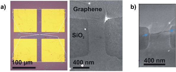
We are investigating graphene as a contact material for molecular electronics. As an alternative to metallic electrodes for molecular junctions, carbon based materials offer great potential to bridge the gap between the macro- and the nanoscale. The two dimensional structure of graphene and the potential to tune it’s charge carrier density, make it a promising material to gain new understanding and control of electronic and optical properties of molecules at room temperature. To achieve reliable and reproducible contacts between molecules and graphene electrodes, the production of nm-size gaps in high quality CVD monolayer graphene are of great interest. We are working on more control of the fabrication of graphene electrode by electro-burning of patterned CVD graphene.
Related publications
-
Thodkar, Kishan, Maria El Abbassi, Felix Lüönd, Frédéric Overney, Christian Schoenenberger, Blaise Jeanneret, and Michel Calame.
physica status solidi (RRL) – Rapid Research Letters 10 (11) , 807-811 (2016) .
![[DOI]](../../wp-content/plugins/papercite/img/external.png)
-
Nef, Cornelia, Laszlo Posa, Peter Makk, Wangyang Fu, Andras Halbritter, Christian Schönenberger, and Michel Calame.
Nanoscale 6 , 7249-7254 (2014) .
-
Fu, W., El M. Abbassi, T. Hasler, M. Jung, M. Steinacher, M. Calame, and C. Schoenenberger.
Appl. Phys. Lett. 104 , 13102 (2014) .
-
Fu, W., C. Nef, A. Tarasov, M. Wipf, R. Stoop, O. Knopfmacher, M. Weiss, M. Calame, and C. Schoenenberger.
Nanoscale 5 , 12104-12110 (2013) .
-
Eren, Baran, Thilo Glatzel, Marcin Kisiel, Wangyang Fu, Rémy Pawlak, Urs Gysin, Cornelia Nef, Laurent Marot, and Michel Calame<em>, et al</em>.
Appl. Phys. Lett. 102 , 71602 (2013) .
-
Fu, Wangyang, Cornelia Nef, Oren Knopfmacher, Alexey Tarasov, Markus Weiss, Michel Calame, and Christian Schoenenberger.
Nano Lett. 11 (9) , 3597-3600 (2011) .
[Abstract]We observe very small gate-voltage shifts in the transfer characteristic of as-prepared graphene field-effect transistors (GFETs) when the pH of the buffer is changed. This observation is in strong contrast to Si-based ion-sensitive FETs. The low gate-shift of a GFET can be further reduced if the graphene surface is covered with a hydrophobic fluorobenzene layer. If a thin Al-oxide layer is applied instead, the opposite happens. This suggests that clean graphene does not sense the chemical potential of protons. A GFET can therefore be used as a reference electrode in an aqueous electrolyte. Our finding sheds light on the large variety of pH-induced gate shifts that have been published for GFETs in the recent literature.